Ddr Ram Circuit Diagram
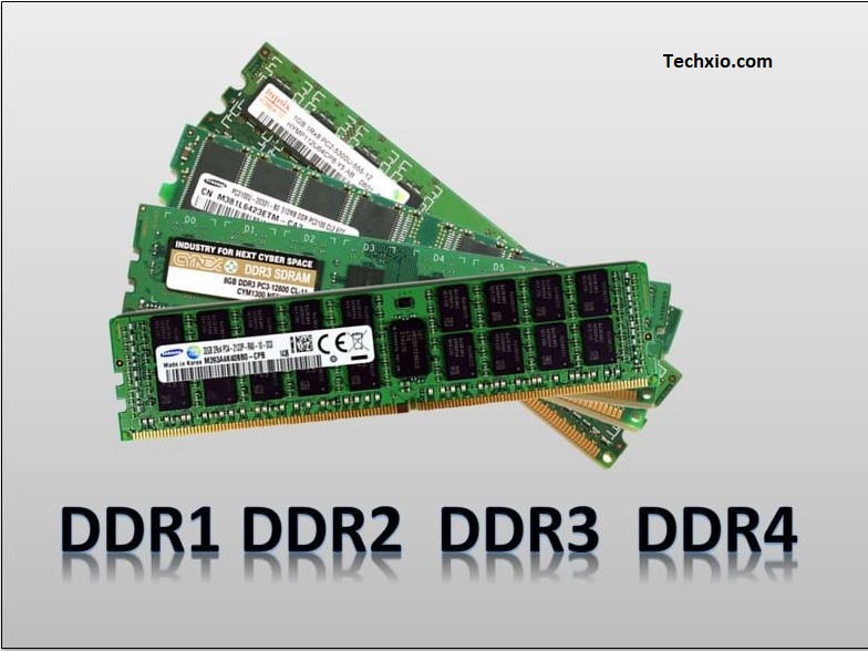
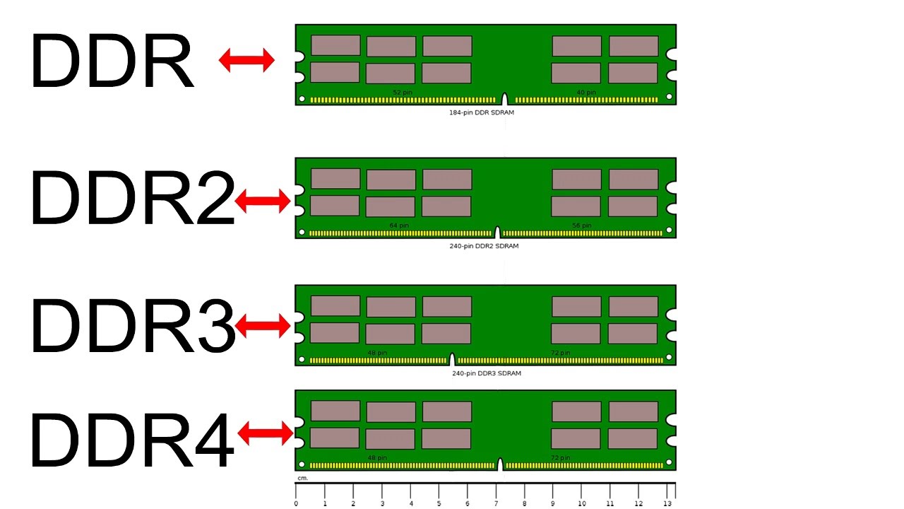
Ram ddr3 ddr4 ddr2 ddr1 physically ddr ddr5 notch mrdustbin Ddr3 pcb Ram read schematic writer circuit circuits seventransistorlabs electronic
PPT - Random-Access Memory (RAM) PowerPoint Presentation, free download
Ram components Ram read/writer Ram components
Ram schaltplan
Ram dimm circuit diagramRam memory cell binary watson write read circuits input access random bc line output latech edu Will ddr5 ram work on ddr4 motherboard? (2023)How to identify ddr1 ddr2 and ddr3 ddr4 ram physically.
Ram circuit diagram for laptop ddr2 ddr3 ddr4 ddr5 ddr1 schematicAm571x support for dual die ddr3 Pcb routing guidelines for ddr memory devices and impedance blogRandom access memory (ram) — sap-1 processor architecture documentation.

Cnc axis4 board schematics (rev. a)
Ddr memory and the challenges in pcb designRam memory structure random access basic write ppt read powerpoint presentation select logic chip data lines address Ram dynamic circuit simulator electronics simulationRam memory structure access random memories.
For the ram circuit above: a)set the dip switch j1 toPcb routing guidelines for ddr4 memory devices Gddr6 vs ddr4 vs hbm2?为什么cpu还不用gddr?异构内存的未来在哪里?Ddr memory-termination supply.

Ram (random access memory) structure
Circuit diagram of ddr2 ramDdr ram circuit diagram Ram dimm circuit diagramDdr termination circuit voltage supply generates figure memory synchronous drams.
Circuit dip switch ram above j1 set chipRam dimm circuit diagram Functional block diagram of ddr sdram controller [2].Circuit diagram of the proposed ram cell.

Project ram.bo32
Circuit diagram of ddr2 ramDdr memory and the challenges in pcb design Rate data diagram double ddr4 vs timing ram ddr using ddr5Ram sap schematic memory access processor architecture random.
Ddr3 schematic datasheet ddr dual e2e ti advise processorsSchematic diagram of 1t rtd-based ram. Audio ram chip memory schematic.Ddr4 fpga clock decoupling pull schematic connected resistors lines layout chip follows.

Ram memory circuit bit cell binary circuits watson figure latech edu
Dynamic ramDdr sdram controller Solved for the schematic diagram below, find (a) the size of.
.

Circuit Diagram Of Ddr2 Ram

Ram Dimm Circuit Diagram

Schematic diagram of 1T RTD-based RAM. | Download Scientific Diagram

Circuit diagram of the proposed RAM cell | Download Scientific Diagram

Ram Dimm Circuit Diagram

RAM Circuit Diagram for Laptop DDR2 DDR3 DDR4 DDR5 DDR1 Schematic
Circuit Diagram Of Ddr2 Ram